Hardware Overview
Design Files
-
Design Files
- Schematic
- KiCad Files
- STEP File
- Board Dimensions:
- 2.50" x 2.00" (635mm x 508mm)
-
Manipulate 3D Model
Controls Mouse Touchscreen Zoom Scroll Wheel 2-Finger Pinch Rotate Left-Click & Drag 1-Finger Drag Move/Translate Right-Click & Drag 2-Finger Drag 
Dimensions of the DAN-F10N GNSS breakout board. Need more measurements?
For more information about the board's dimensions, users can download the KiCad files for this board. These files can be opened in KiCad and additional measurements can be made with the measuring tool.
KiCad - Free Download!
KiCad is free, open-source CAD program for electronics. Click on the button below to download their software. (*Users can find out more information about KiCad from their website.)
 Measuring Tool
This video demonstrates how to utilize the dimensions tool in KiCad, to include additional measurements:

Board Layout
The SparkFun Dualband L1/L5 GNSS Breakout - DAN-F10N features the following:

Layout of the major components on the breakout board.
-
- USB-C Connector
- The primary inteface for powering and interacting with the board
-
- DAN-F10N GNSS Module
- The u-blox DAN-F10N GNSS module
-
- Headers
- Exposes pins to power the board and breaks out the pins of the DAN-F10N GNSS module
-
- Status LEDs
- LED status indicators for the DAN-F10N GNSS module
-
L1/L5 AntennaU.FL Connector- An optional input for an external GNSS antenna
-
- Backup Battery
- Backup power to maintain ephemeris data on the DAN-F10N GNSS module for warm starts
Power
The simplest method to power the board is through the USB-C connector. However, the DAN-F10N Dualband L1/L5 GNSS breakout board only requires 3.3V, which can be supplied though the PTH pins.

DAN-F10N Dualband L1/L5 GNSS breakout board's power connections.
Below, is a general summary of the power circuitry on the board; most are broken out as PTH pins:
5V- The voltage from the USB-C connector, usually 5V.- Input Voltage Range: 1.2 - 5.5V (1)
- Power source for the entire board
- Powers the 3.3V voltage regulator (RT9080), which can source up to 600mA
- When enabled, it can also power the BlueSMiRF header
3V3- Provides a regulated 3.3V from the RT9080, using the power supplied from the5Vpin or USB-C connector.- Used to power the DAN-F10N module, power LED, and backup battery
- Controlled by the
ENpin, which is enabled by default
EN- Controls the 3.3V voltage regulator RT9080, enabling the voltage output (activeHIGH)RST- Used to reset the DAN-F10N GNSS module- Connected to the
RESET_Npin of the DAN-F10N module, an input-only pin with an internal pull-up resistor (2) - Driving the pin
LOWfor at least 1ms triggers a cold-start reset, clearing theBBRcontent (receiver configuration, real-time clock (RTC), and GNSS orbit data)
- Connected to the
GND- The common ground or the 0V reference for the voltage supplies.- Backup Battery - Provides backup power to the DAN-F10N GNSS module to maintain ephemeris data for warm starts
-
While the RT9080 LDO regulator has an input voltage range of 1.2 - 5.5V, a minimum supply voltage of 3.5V is recommended for a 3.3V output.
-
No capacitors should be placed between
RESET_Nto GND, otherwise it could trigger a reset on every startup.
JST Connector
The 3V3 pin of the BlueSMiRF header is designed to operate as a voltage output. However, an input voltage can be supplied through the pin, but users should be mindful of any voltage contention issues.
Info
For more details, users can reference the schematic and the datasheets of the individual components on the board.
Power Modes
The DAN-F10N GNSS module supports three different operation modes:
- Continuous Mode
-
In this mode, the module uses dedicated signal processing engines optimized for signal acquisition and tracking.
- The acquisition engine actively searches and acquires signals, during cold starts or when insufficient signals are available during navigation.
- The tracking engine continuously tracks signals, downloads all the almanac data, and acquires new signals as they become available during navigation.
The tracking engine consumes less power than the acquisition engine. Therefore, the module's current consumption is lower when a valid position is obtained quickly after startup, the entire almanac has been downloaded, and the ephemeris for available satellites are valid.
- Backup Modes
-
The DAN-F10N module supports two backup modes. The backup modes are inactive states with reduced power consumption, where the receiver maintains time, information, and navigation data to speed up signal acquisitions upon restart.
- Hardware backup mode
- The hardware backup mode requires
V_BCKPpower to be supplied. It allows the module to enter a backup state and maintain the backup domain (BBRandRTC), after the main power has been switched off.
- Software standby mode
- Software standby mode is entered using the
UBX-RXM-PMREQmessage. This mode will clear the RAM memory; to maintain the receiver configuration, it should be stored onBBRor flash layers. The software standby mode can be set for a specific duration, or until the receiver is woken up by a signal from the UARTRXand/orEXTINTpins, as defined inUBX-RXM-PMREQmessage. A system reset with theRESET_Nsignal also terminates the software standby mode, clears theBBRcontent and restarts the receiver.
Power Consumption
The power consumption of the DAN-F10N module depends on the GNSS signals enabled and if the module is acquiring or tacking those signals. The table below, lists the average current consumption with a supply voltage of 3.3V.
| GNSS Signals | Acquisition | Tracking |
|---|---|---|
| GPS+GAL+BDS | 26mA | 21mA |
| GPS+BDS | 26mA | 20mA |
| GPS+GAL | 22mA | 19mA |
| GPS+NavIC | 21mA | 18mA |
| GPS | 20mA | 18mA |
| BDS | 24mA | 19mA |
Tip
At startup, the inrush current can reach up to 100 mA at startup. Make sure the primary power source can sustain the required current consumption.
Backup Modes
The current consumption for the backup modes:
- Hardware backup Mode: 31µA
- Software standby Mode: 49µA
Info
For more information, please refer to the DAN-F10N Datasheet.
DAN-F10N GNSS Receiver
The centerpiece of the DAN-F10N Dualband L1/L5 GNSS breakout board, is the DAN-F10N module from u-blox. Their proprietary dual-band multipath mitigation technology enables the u-blox F10 GNSS engine to isolate the best signals from the L1 and L5 bands; delivering a solid meter-level position accuracy in challenging urban environments. Additionally, the DAN-F10N module's robust SAW-LNA-SAW RF architecture with an additional notch filter on the L1 RF path ensures the best possible out-of-band interference mitigation from nearby cellular modems.
The DAN-F10N GNSS module comes with a 20 x 20 x 8 mm, integrated, Right Hand Circular Polarized (RHCP), L1/L5 dual-band patch antenna that offers the best compromise between size and performance. The patch antenna's wide beamwidth provides flexibility in the device's orientation; while alternatively, the module also has an antenna switch function to give users the option to utilize an external dual-band antenna, further increasing its utility.


The DAN-F10N module on the breakout board.
Features:
- Operating Voltage: 2.7 - 3.6V
- Operating Temperature: -40 - 85°C
- GNSS Support
- GPS: L1 C/A, L5
- QZSS: L1C/A, L1S, L1Sb, L5
- GAL: E1B/C, E5a
- BDS: B1C, B2a
- NavIC: L5
- SBAS: L1C/A
- BDSBAS: B1C
- Sensitivity
- Tracking & Nav: –164dBm
- Reacquisition: –156dBm
- Cold start: –145dBm
- Hot start: –156dBm
- Update Rate: Up to 10Hz
- Time to Fix
- Cold Start: < 28s
- Aided Start: < 2s
- Hot Start: 2s
- Position Accuracy
- 1.0 m (with SBAS)
- 1.5 m (without SBAS)
- Interfaces
- 1x Serial interface
- Raw data output: Code phase data
- Protocols: NMEA 4.11, UBX binary
- 2x Digital I/O
- Timepulse Configurable: 0.25 - 10MHz
EXTINTinput for Wakeup
- 1x Serial interface
Frequency Bands
The DAN-F10N GNSS module is a dual-band, multi-constellation GNSS receiver. Below, are the frequency bands provided by all the global navigation satellite systems and the ones supported by the DAN-F10N module.
| Constellation | Frequency Bands |
|---|---|
| GPS | L1 C/A, L5 |
| QZSS | L1C/A, L1S, L1Sb, L5 |
| GAL | E1B/C, E5a |
| BDS | B1C, B2a |
| NavIC | L5 |
| SBAS | L1C/A |
| BDSBAS | B1C |
The frequency bands supported by the DAN-F10N GNSS receiver.
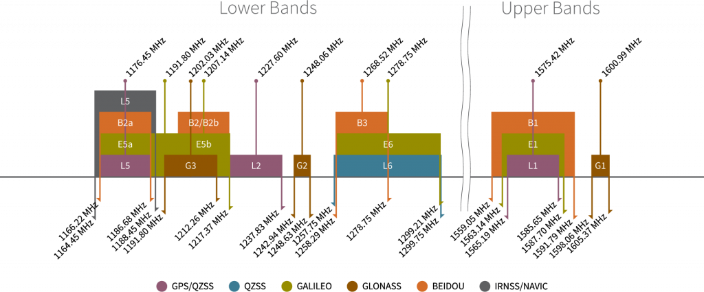
Frequency bands of the global navigation satellite systems. (Source: Tallysman)
What are Frequency Bands?
A frequency band is a section of the electromagnetic spectrum, usually denoted by the range of its upper and lower limits. In the radio spectrum, these frequency bands are usually regulated by region, often through a government entity. This regulation prevents the interference of RF communication; and often includes major penalties for any interference with critical infrastructure systems and emergency services.

However, if the various GNSS constellations share similar frequency bands, then how do they avoid interfering with one another? Without going too far into detail, the image above illustrates the frequency bands of each system with a few characteristics specific to their signals. Wit these characteristics in mind, along with other factors, the chart can help users to visualize how multiple GNSS constellations might co-exist with each other.
For more information, users may find these articles of interest:
Peripherals and I/O Pins
The DAN-F10N module has twelve I/O pins, of which five are programmable. Most of these are broken out as PTH pins on the DAN-F10N Dualband L1/L5 GNSS breakout board; whereas, others are broken out to their specific interface (i.e. USB connector, jumper, U.FL connector, etc.). Additionally, some of the I/O connections are broken out with multiple components or interfaces.

The UART interfaces on the DAN-F10N GNSS breakout board.

The I/O pins on the DAN-F10N GNSS breakout board.
Interfaces:
- 1x UART
1x LNA enable pin(1)- 1x External interrupt
- 1x PPS output signal
- 1x Safe boot pin
- 1x Reset pin
- Not available on the DAN-F10N Dualband L1/L5 GNSS breakout board.

COM pins on the DAN-F10N GNSS breakout board.
The DAN-F10N has a single UART interface that can be accessed either through the PTH pins or the USB-C connector, with the help of the CH340 USB-to-serial converter. The operation of these connections is configured with the RX and TX jumpers.
Supported Protocols
The UART interface supports the following protocols:
- Input messages: NMEA and UBX
- Output messages: NMEA (GGA, GLL, GSA, GSV, RMC, VTG, and TXT)
Configuration Settings
The UART interface can be configured with the CFG-UART1-* messages, but will initially have the following settings:
- Baudrate: 9600 to 921600bps (Default: 38400bps)
- Data Bits: 8
- Parity: No
- Stop Bits: 1
- Flow Control: None

GPx pins on the DAN-F10N GNSS breakout board.
The DAN-F10N module features five programmable I/O pins, but the LNA enable pin is not broken out on this board. All the inputs have internal pull-up resistors in normal operation and can be left open if unused.
-
EXTINT- DAN-F10N supports external interrupts through its
EXTINTpin. This is useful for waking the module up from its standby mode or for timing applications.
-
SBT(Reserved for future use)- The
SAFEBOOT_Npin is for updates and reconfiguration. The DAN-F10N module will enter safeboot mode, if this pin is pulledLOWat starup.
-
PPS-
The
PPSpin is connected to theTIMEPULSEpin of the DAN-F10N and thePPSLED. The period, length, and polarity (rising or falling edge) of theTIMEPULSEsignal can be configured with theCFG-TP-*messages.Info
The
SBT(SAFEBOOT_N) andPPS(TIMEPULSE) pins are internally connected in the DAN-F10N module, by a 1 kΩ series resistor. Make sure these pins have no load that could pull them low at startup; otherwise, the receiver will enter its safeboot mode.
-
RST-
The
RSTpin is connected to theRESET_Npin of the DAN-F10N module. Driving the pinLOWfor at least 1ms triggers a cold-start reset, clearing theBBRcontent (receiver configuration, real-time clock (RTC), and GNSS orbit data).Info
Capacitors should not be placed between
RSTandGND; otherwise, it could trigger a reset on startup.

PPS output signal on the DAN-F10N GNSS breakout board.
The PPS pin is connected to the module's time pulse (TIMEPULSE) signal and the PPS LED, as a visual indicator. The period, length, and polarity (rising or falling edge) of the TIMEPULSE signal can be configured with the CFG-TP-* messages.
Disable LED
There is a jumper attached to the PPS LED. For low power applications, users can cut the jumper to disable the PPS LED.
Info
The module's SAFEBOOT_N (SBT) pin is internally connected to its TIMEPULSE (PPS) pin through a 1 kΩ series resistor. Make sure these pins have no load that could pull them low at startup; otherwise, the receiver will enter its safeboot mode.
USB-C Connector
A USB connector is provided to power the board and interface with the DAN-F10N GNSS receiver through a CH340 USB-to-serial converter. For most users, it will be the primary method for communicating with the DAN-F10N module.

USB-C connector on the DAN-F10N GNSS breakout board.
Info
Users will need to install the USB driver for the CH340 USB-to-serial converter, before they can interact with the DAN-F10N GNNS module.
U.FL Connector
The L1/L5 Antenna U.FL connector provides an optional, input for a external GNSS antenna. Users will need to modify the EXT_ANT jumper, to trigger the RF switch to change from the integrated patch antenna to the external antenna connection.

The U.FL connector to attach an external GNSS antenna to the DAN-F10N GNSS breakout board.
Tip
For the best performance, we recommend users choose a compatible L1/L5 GNSS antenna and utilize a low-loss cable. Also, don't forget that GNSS signals are fairly weak and can't penetrate buildings or dense vegetation. The GNSS antenna should have an unobstructed view of the sky.
BlueSMiRF Header
The DAN-F10N has a single UART interface that can be accessed either through the BlueSMiRF header pins or the USB-C connector. The BlueSMiRF header can be used to connect the DAN-F10N GNSS module to external devices, such as a microcontroller or BlueSMiRF v2, Bluetooth® serial link.

The BlueSMiRF header pins on the DAN-F10N GNSS breakout board.
Supported Protocols
The UART interface supports the following protocols:
- Input messages: NMEA and UBX
- Output messages: NMEA (GGA, GLL, GSA, GSV, RMC, VTG, and TXT)
Configuration Settings
The UART interface can be configured with the CFG-UART1-* messages, but will initially have the following settings:
- Baudrate: 9600 to 921600bps (Default: 38400bps)
- Data Bits: 8
- Parity: No
- Stop Bits: 1
- Flow Control: None
Bus Contention
To avoid bus contention issues between the USB-C connection and the external device, users may want to use the RXD and TXD jumpers to disconnect the CH340 USB-to-serial converter from the UART interface of the DAN-F10N GNSS module.
Pin Connections
When connecting the DAN-F10N Dualband L1/L5 GNSS breakout board to another device, users need to be aware of the pin connections and voltage ranges of the products. Below, is a table of the pin connections for the BlueSMiRF header pins on the DAN-F10N GNSS breakout board.
| Pin Number |
1 (Left Side) |
2 | 3 | 4 | 5 |
6 (Right) |
|---|---|---|---|---|---|---|
| Label | NC |
TXD |
RXD |
3V3 |
NC |
GND |
| Function | UART - Transmit | UART - Receive | Output Voltage: 3.3V | Ground |
Status LEDs

The status indicator LEDs on the DAN-F10N Dualband L1/L5 GNSS breakout board.
There are two status LEDs on the DAN-F10N Dualband L1/L5 GNSS breakout board:
PWR- Power (Red)- Turns on once 3.3V power is supplied to the board
PPS- Pulse-Per-Second (Green)- Indicates when there is a time pulse signal (see the PPS Output section)
Info
For low power applications, the LEDs can be disabled to conserve energy. See the Jumpers section.
Jumpers
Never modified a jumper before?
Check out our Jumper Pads and PCB Traces tutorial for a quick introduction!
-

How to Work with Jumper Pads and PCB Traces
There are seven jumpers on the back of the board that can be used to easily modify the hardware connections on the board.

The jumpers on the bottom of the DAN-F10N Dualband L1/L5 GNSS breakout board.
- LED Jumpers
-
Two of the jumpers control power to the status LEDs on the board.
Info
By default, all the jumpers are connected, to power the status LEDs. For low power applications, users can cut the jumpers to disconnect power from each of the LEDs.
PWR- This jumper can be cut to remove power from the red, power LED.PPS- This jumper can be cut to remove power from the green,PPSLED that is provided by thePPSsignal.
- UART Jumpers
-
Two of the jumpers control the
RXandTXsignals on the board.Tip
A 1kΩ resistor is placed on the
RXD- This jumper can be cut to disconnect theRXsignal of the DAN-F10N module from the CH340 USB-to-serial converter.TXD- This jumper can be cut to disconnect theTXsignal of the DAN-F10N module from the CH340 USB-to-serial converter.
EXT_ANT-
This jumper can be modified to control the source of the GNSS signals between the DAN-F10N module's integrated L1/L5 dual-band patch antenna or an external antenna connected to the board's U.FL connector.
Info
By default, the module's integrated L1/L5 dual-band patch antenna is utilized.
MEAS- This jumper can be cut for current measurments to the RT9080 voltage regulator from the USB-C connector or
5Vpin. SHLD- This jumper can be cut to disconnect the shield of the USB-C connector from the board's ground plane.