Hardware Overview
Important: Read Before Use!
ESD Sensitivity
The mosaic-T module is sensitive to ESD. Use a proper grounding system to make sure that the working surface and the components are at the same electric potential.
ESD Precaution
As recommended by the manufacturer, we highly recommend that users take the necessary ESD precautions to avoid damaging their module.

-

iFixit Anti-Static Wrist Strap
TOL-25572
Active Antenna
Never inject an external DC voltage into the SMA connector for the GNSS antenna, as it may damage the mosaic-T module. For instance, when using a splitter to distribute the antenna signal to several GNSS receivers, make sure that no more than one output of the splitter passes DC. Use DC-blocks otherwise.
External Reference Clock
If the switch for an external reference clock is enabled, users must provide a 10MHz input signal. Otherwise, the mosaic-T module will cease to operate, without a clock signal.
Design Files
-
Design Files
- Schematic
- KiCad Files
- STEP File
- Board Dimensions:
- 2.50" x 2.00" (635mm x 508mm)
-
Manipulate 3D Model
Controls Mouse Touchscreen Zoom Scroll Wheel 2-Finger Pinch Rotate Left-Click & Drag 1-Finger Drag Move/Translate Right-Click & Drag 2-Finger Drag 
Dimensions of the mosaic-T Timing GNSS breakout board. Need more measurements?
For more information about the board's dimensions, users can download the KiCad files for this board. These files can be opened in KiCad and additional measurements can be made with the measuring tool.
KiCad - Free Download!
KiCad is free, open-source CAD program for electronics. Click on the button below to download their software. (*Users can find out more information about KiCad from their website.)
 Measuring Tool
This video demonstrates how to utilize the dimensions tool in KiCad, to include additional measurements:

Board Layout
The SparkFun Timing GNSS Breakout - mosaic-T features the following:

Layout of the major components on the breakout board.
-
- USB-C Connector
- The primary inteface for powering and interacting with the board
-
- 6-Pin JST Connector
- A UART interface for the mosaic-T GNSS module
-
- µSD Card Slot
- An SD card slot for data logging
-
LOGButton- A button to mount the SD card and intialize the data logging stream
-
- mosaic-T GNSS Module
- The Septentrio mosaic-T GNSS module
-
- Status LEDs
- LED status indicators for the mosaic-T GNSS module
- SMA Connectors
L1/L2/L5/L: The input for a GNSS antennaEXT REF: The input for an external reference clock signal
-
INT/EXTSwitch- Used to switch between an internal or external refernce clock signal for the mosaic-T GNSS module. If switched to
EXT, an external 10MHz signal must be provided for the GNSS module to function
USB-C Connector
A USB connector is provided to power and interface with the mosaic-T GNSS receiver. For most users, it will be the primary method for communicating with the mosaic-T module.

USB-C connector on the mosaic-T Timing GNSS breakout board.
Windows OS
For Windows computers, users will need to install the USB driver before they can interact with the mosaic-T GNNS module.
Info
For more details about this interface, please refer to the USB-C Connector section below.
Power
The simplest method to power the board is through the USB-C connector. However, the mosaic-T Timing GNSS breakout board only requires 3.3V to power most of its components(1), which can be supplied though JST connector or PTH pins.
- 5V is only required to utilize the USB interface; and when enabled, it can also power the JST connector.

mosaic-T Timing GNSS breakout board's power connections.
Below, is a general summary of the power circuitry on the board, broken out as PTH pins:
VUSB- The voltage from the USB-C connector, usually 5V.- Input Voltage Range: 2.2 - 5.5 V
- Power source for the entire board.
- Powers the 3.3V voltage regulator (AP7361C) and when enabled, it can also power the JST connector. (1)
- This pin powers the integrated PHY of the mosaic-T module's USB interface.
VIN- Alternate input supply voltage for the board.- Input Voltage Range: 2.2 - 6 V
- Alternative power supply input for the board, excluding the integrated PHY of the USB interface.
- Powers the 3.3V voltage regulator (AP7361C) and when enabled, it can also power the JST connector. (2)
3V3- Provides a regulated 3.3V from AP7361C using the power from theVINorVUSB(5V) inputs.- Input Voltage Range: 3.135 - 3.465 V
- The 3.3V AP7361C LDO regulator can source up to 1A.
- Used to power the mosaic-T module, SD card slot, power LED, and the active antenna preamplifier for the mosaic-T module.
VBATT- Always-on power supply- Input Voltage Range: 3.135 - 3.465 V
- Tied to
3.3V(see the Jumpers section).- Used to power the module in Standby mode.
GND- The common ground or the 0V reference for the voltage supplies.
- While the AP7361C LDO regulator has an input voltage range of 2.2 - 6V, users should supply:
- A minimum of 3.5V for a 3.3V output from the regulator
- A maximum of 5.5V as not to exceed the electrical limitations of the mosaic-T module
- While the AP7361C LDO regulator has an input voltage range of 2.2 - 6V, a minimum supply voltage of 3.5V is recommended for a 3.3V output.
JST Connector
The V pin of the JST connector is designed to operate as a voltage output. However, an input voltage can be supplied through the connector, but users should be mindful of any voltage contention issues.
Info
For more details, users can reference the schematic and the datasheets of the individual components on the board.
Power Modes
The mosaic-T module operates in three different power states, which

The power management pins of the mosaic-T Timing GNSS breakout board.
- Off - The module is completely turned off
- When transitioning to the Off state from Active, recent data may not be lost and not logged to the external SD card
- Standby - The module is in a low-power consumption mode (1)
- The module power consumption in standby is <5mW
- The
PMICpin is drivenLOW - The
RDYpin is in aLOW - When the
ON OFFpin is drivenLOWfor at least 50ms, the module toggles between its Standby and Active states
- Active - The module is operating with all functions active
- On power up, the module restarts in the configuration stored in the boot configuration file
- The
PMICpin is drivenHIGH - The
RDYpin is in aHIGH(2)
- Essentially, the same state as Off; except in the transition to the Standby mode, before the module shuts down:
- All logging tasks are terminated
- The SD card is unmounted
- The
PMICpin is drivenLOW
- Level becomes
HIGHabout 300ms after powering up, reset, or waking up from standby
Info
For more information on the power management of the mosaic-T module, please refer to sections 3.4, 3.5, 4.1, and 4.13 of the hardware manual.
Drive Current
The drive current on the PMIC, RDY, and ON OFF pins is minimal. Enough to be read by a digital pin on a microcontroller, but not high enough to drive an LED.
Power Consumption
The power consumption of the mosaic-T module depends on the GNSS signals enabled and the positioning mode. The table below, lists the average power consumption for common configurations. The current listed, is based on a supply voltage of 3.3V.
| GNSS Signals | Positioning Mode | Power (mW) | Current (mA) |
|---|---|---|---|
| GPS L1 C/A | Stand-Alone (1Hz) | 550 | 167 |
| GPS L1/L2 | RTK (1Hz) | 670 | 203 |
| GPS/GLONASS L1/L2 | RTK (1Hz) | 695 | 211 |
| GPS/GLONASS L1/L2+GALILEO L1/E5a +BeiDou B1C/B2a | RTK (1Hz) | 850 | 258 |
| GPS/GLONASS L1/L2+GALILEO L1/E5a +BeiDou B1C/B2a | RTK (100 Hz) | 930 | 282 |
| GPS/GLONASS L1/L2 + L-band | PPP (1Hz) | 760 | 230 |
| All signals from all GNSS constellations | Static (1Hz) | 910 | 276 |
| All signals from all GNSS constellations +L-band | Static(1Hz) | 980 | 297 |
| All signals from all GNSS constellations +L-band | Static (100Hz) | 1080 | 327 |
Source: mosaic-T Hardware Manual
mosaic-T
The centerpiece of the mosaic-T Timing GNSS breakout board, is the mosaic-T module from Septentrio. Their mosaic modules are low-power, multi-band, multi-constellation GNSS receivers capable of delivering centimeter-level precision at high update rates. The modules also feature Septentrio's unique AIM+ technology for interference mitigation and anti-spoofing, which ensures their best-in-class reliability and scalable position accuracy.

RTK Not Supported
The mosaic-T is a superb GNSS module designed for highly accurate timing applications. But it does not support RTK. It can not be configured as a RTK Rover or Base. RTCM output is not supported.

The mosaic-T module on the mosaic-T Timing GNSS breakout board.
Features:
- Operating Voltage: 3.135 - 3.465V
- Operating Temperature: -40 - 85°C
- GNSS Support
- GPS: L1C/A, L1PY, L2C, L2P, L5
- GLONASS: L1CA, L2CA, L2P, L3 CDMA
- Beidou: B1I, B1C, B2a, B2b, B2I, B3
- Galileo: E1, E5a, E5b, E5 AltBoc, E6
- QZSS: L1C/A, L1 C/B, L2C, L5
- Navic: L5
- SBAS: Egnos, WA
- Antenna Specifications
- Preamplification Range: 15-50dB
- Bias Voltage: 3.0 - 5.5V
- 448 Hardware Channels
- Update Rate: 100Hz
- Latency: < 10ms
- Time to Fix
- Cold Start: < 45s
- Warm: < 20s
- Reacquisition: 1s
- Timing Precision: 5ns
-
Position Accuracy
Correction Horizontal Vertical DGNSS 40cm
~1.3'70cm
~2.3'SBAS 60cm
~2'80cm
~2.6'Standalone 1.2m
~4'1.9m
~6.2'
Info
The mosaic-T has three power modes: Active, Standby, and Off (see the Power Modes section).
Frequency Bands
The mosaic modules are multi-band, multi-constellation GNSS receivers. Below, are charts illustrating the frequency bands utilized by all the global navigation satellite systems and the ones supported by the mosaic-T module.

The frequency bands supported by the mosaic-T GNSS receiver.
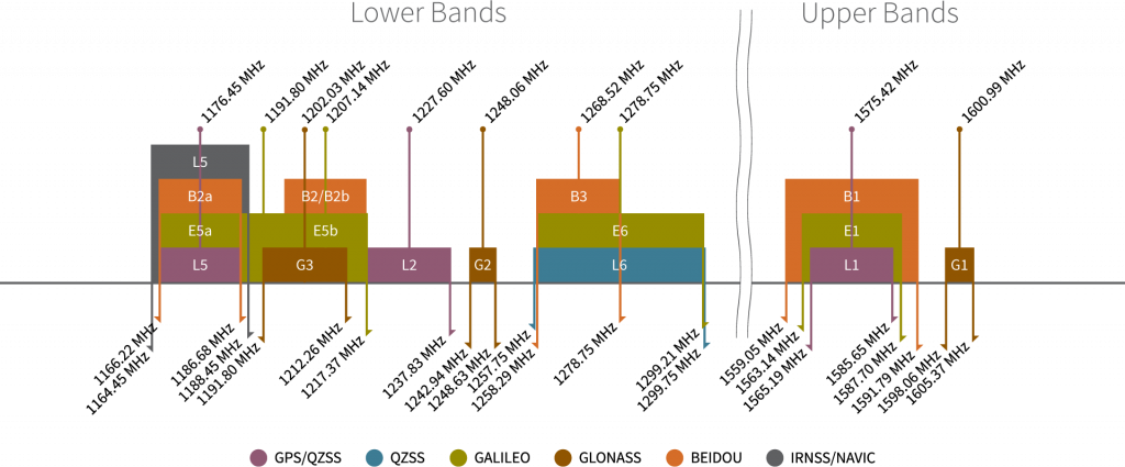
Frequency bands of the global navigation satellite systems. (Source: Tallysman)
Info
For a comparison of the frequency bands supported by the mosaic modules, refer to section 3.1 of the hardware manual.
What are Frequency Bands?
A frequency band is a section of the electromagnetic spectrum, usually denoted by the range of its upper and lower limits. In the radio spectrum, these frequency bands are usually regulated by region, often through a government entity. This regulation prevents the interference of RF communication; and often includes major penalties for any interference with critical infrastructure systems and emergency services.

However, if the various GNSS constellations share similar frequency bands, then how do they avoid interfering with one another? Without going too far into detail, the image above illustrates the frequency bands of each system with a few characteristics specific to their signals. Wit these characteristics in mind, along with other factors, the chart can help users to visualize how multiple GNSS constellations might co-exist with each other.
For more information, users may find these articles of interest:
Position Accuracy
RTK Not Supported
The mosaic-T is a superb GNSS module designed for highly accurate timing applications. But it does not support RTK. It can not be configured as a RTK Rover or Base. RTCM output is not supported.
Tip
For the best performance, we highly recommend that users select a compatible L1/L2/L5 (tri-band) GNSS antenna and utilize a low-loss cable.
Peripherals and I/O Pins
The mosaic-T features several peripherals and I/O pins. Some of these are broken out as pins on the mosaic-T Timing GNSS breakout board; whereas, others are broken out to their specific interface (i.e. µSD Carsd slot, USB connector, etc.). Additionally, some of the pin connections are shared with other components or interfaces.

The I/O pins on the mosaic-T Timing GNSS breakout board.

The peripheral interfaces of the mosaic-T Timing GNSS breakout board.
Interfaces:
- 4x UART (LVTTL, up to 4 Mbps)
Ethernet (RMII/MDIO), 10/100 Mbps(1)- USB device (2.0, HS)
- SDIO (mass storage)
- 2x GPIO user programmable
- 2x Event markers
- 1x Configurable PPS out
- Not available on the mosaic-T Timing GNSS breakout board.
I/O Pins
There are thirty I/O pins on the mosaic-T Timing GNSS breakout board, most of which are connected to other interfaces and components of the board. The tabulated section below, details the aspects of each pin based on their function.

COM pins on the mosaic-T Timing GNSS breakout board.
The mosaic-T has four UARTs that are organized into separate COM ports, three of which are available through PTH pins. The operation for each of these ports can be configured separately.
COMports 1-3 feature flow control pins, which are disabled by default.- These ports also support a point-to-point protocol server, by which it can accept TCP/IP connections over a serial link.
Info
By default, the COM ports will be configured with the following settings:
- Baudrate: 115200bps
- Data Bits: 8
- Parity: No
- Stop Bits: 1
- Flow Control: None
Where is COM3?
COM3 is available through the JST connector, but the pins can also be accessed from the pads on the bottom of the board.
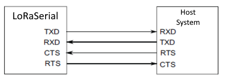
Pin Connections
When connecting to the board's UART pins, the pins should be connected based upon the flow of their data. For example, when utilizing the Telemetry Radio or the LoRaSerial Kit:

PPS output signal on the mosaic-T Timing GNSS breakout board.
From the module, the PPS output signal's logic-level is 1.8V. However, for the convenience of users, we have added a buffer and bumped up the signal's logic-level to 3.3V on the mosaic-T Timing GNSS breakout board. This 3.3V signal output can be access through the PPS pin. The signal is also connected to the PPS LED, to be used as a visual indicator.
Disable LED
There is a jumper attached to the PPS LED. For low power applications, users can cut the jumper to disable the PPS LED.
Use Case
- Users could use this signal in conjunction with the event pins to synchronize two mosaic-T modules with each other.
- Users could use this signal to create their own Stratum 0 source for the NTP on a primary time server.

The data logging functionality of the board can be configured through the software/web interfaces and operated through the use of the LOG button or LOG BTN pin. Data logging activity will be indicated by the LOG LED.
LOG BTN- Connected to the LOG button and tied to the same active-high, input of the mosaic-TLOG- Connected to theLOGLED
Initial Configuration
Before data logging can occur, it is necessary to create a logging stream from the Logging tab of the web interface or using the RxTools software suite. Streams can contain NMEA or SBF (Septentrio Binary Format) data; SBF can contain RTCM and/or RINEX. (see the Data Logging section)
Operation
The data logging feature can be controlled on the board through either the LOG button or LOG BTN pin.
- Pressing the button or pin
LOW(< 5s) toggles data logging to the SD card on and off. - Holding the button or pin
LOWfor more than 5 seconds (> 5s) and then releasing it, will force the board to:- Unmount the SD card if it was mounted
- Mount the SD card if it was unmounted
Status
The status of the SD card and data stream are indicated on the LOG LED and pin.
| Pin | LED | Status |
|---|---|---|
| Low | Off | SD card not present or unmounted |
| High | On | SD card present and mounted |
| Pulses | Blinking | Data logging activity |

The mosaic-T module features two general purpose, output LED pins. These pins have a maximum output current of 10 mA and output impedance of 20Ω. In addition, to these pins, there are other status LEDs connected to other signals on the board.
- The general purpose LED signals are connected to the
RTKandPVTpins; and respectively, theRTKandPVTLEDs. - The PPS output signal is connected to the
PPSpin andPPSLED. - The
LOGpin is connected to theLOGLED.
Info
For more details, please refer to the Status LEDs section.
The mosaic-T module features two general purpose, output pins. These pins can drive a maximum current of 10mA.

GPx pins on the mosaic-T Timing GNSS breakout board.
The mosaic-T module features two general purpose, event input pins. These pins can be used to time tag external events with a time resolution of 20ns.

Example
For example, these pins can be used in conjunction with the PPS output signal for time syncing.

Reset
-
ResetPin- Used to reset the mosaic-T module.
Power Mode
Info
For more details, please refer to the Power Modes section.
-
RDYPin- The
RDYpin indicates the operational mode of the mosaic-T module. The level is high when module is operating, and low when in standby or reset.
-
PMICPin- The
PMICpin is typically connected to a power switch or the control pin for the primary power supply, which is used to transition the module between its Active and Standby states.
-
ON OFFPin- When the
ONOFFpin is drivenLOW(>50ms), the module toggles between its Active and Standby states.

Info
For more details, please refer to the Power section.
-
VBATTPin- Always-on power supply, which must remain available when 3V3 is disable, by the
PMICpin
-
VUSBPin- The voltage from the USB-C connector, usually 5V
-
VINPin- Alternate input supply voltage for the board
-
3V3Pin- Main power supply input, controlled by the external power switch
-
GNDPin- The common ground or the 0V reference for the voltage supplies
USB-C Connector
For most users, this will be the primary interface for the mosaic-T module.
USB-C connector on the mosaic-T Timing GNSS breakout board.
- When the board is initially connected to a computer, the module will initialize as a USB mass storage device.
- For Windows PCs, the USB driver can be installed from the mass storage device or the RxTools software suite.
- When the SD card is mounted, this drive will contain the contents of the SD card that is inserted on the board.
- Once the USB driver is installed:
- Two virtual
COMports are emulated, which can be used as standard serial interfaces to access the receiver. - This interface will support Ethernet-over-USB.
- By default, the receiver is not allowed to access the Internet over USB.
- The IP address allocated to the Ethernet-over-USB interface is
192.168.3.1.- The IP address cannot be changed; therefore, only single receiver should be connected to your computer at a time.
- Two virtual
SMA Connectors
There are two SMA connectors on the mosaic-T Timing GNSS breakout board.
L1/L2/L5/L
The L1/L2/L5/L SMA connector provides an input for a compatible GNSS antenna. The type of antenna used with the mosaic-T module will affect the overall performance of the GNSS receiver.

The SMA connector to attach a GNSS antenna to the mosaic-T Timing GNSS breakout board.
There are some key parameters related to an antenna that can make or break the signal reception from the satellites. These include the operation frequency, gain, polarization, efficiency, and overall loss.
-
An active antenna often features a LNA. This allows the module to boost the signal received by the GNSS module without degrading the SNR.
- The connector already provides active power at 3.3V.
Danger
Never inject an external DC voltage into the SMA connector for the GNSS antenna, as it may damage the mosaic-T module. For instance, when using a splitter to distribute the antenna signal to several GNSS receivers, make sure that no more than one output of the splitter passes DC. Use DC-blocks otherwise.
-
The more frequency bands an antenna supports, often equates to a gain in the performance.
- Faster acquisition time.
- Access and support for the
L5GPS band can potentially mitigate multi-path errors. - Less susceptible to jamming and spoofing.
Tip
For the best performance, we recommend users choose a compatible L1/L2/L5/L-band GNSS antenna and utilize a low-loss cable. Also, don't forget that GNSS signals are fairly weak and can't penetrate buildings or dense vegetation. The GNSS antenna should have an unobstructed view of the sky.
EXT REF
The primary feature of the mosaic-T is that it can be utilized to create a GNSS disciplined oscillator and calibrate an external reference clock to an accuracy of 20ns.

The JST connector on the mosaic-T Timing GNSS breakout board.
-
The
INT/EXTslide switch selects a reference clock source from either:- The internal TCXO of the mosaic-T module
- An external clock signal from the
EXT REFSMA connector
Warning
If the reference clock switch is set to
EXT, users must provide a 10MHz input signal. Otherwise, the mosaic-T module will cease to operate, without a clock signal. Additionally, switching between external and internal frequency reference must occur when the module is powered off, or the module must be reset after switching. -
The
EXT REFSMA connector accepts a 50Ω, 10MHz signal with the following requirements:- Preferably a sine wave or a band-limited square wave
- Power: -14dBm (min); +14dBm (max)
- Frequency tolerance: +/-2.5ppm
- Allan variance: better than 1ppb (for τ=1s)
- Phase noise: better than -90dBc/Hz at an offset of 10Hz
Tip
If a CMOS or LVTTL signal is used with long traces from the source, it is recommended to filter them at the source with an RC filter with a pole near 100 MHz.
JST Connector
The mosaic-T Timing GNSS breakout board features a 6-pin JST GH connector, which is polarized and locking. Users can access the COM3 port of the mosaic-T module through the JST connector with our breadboard cable.

The JST connector on the mosaic-T Timing GNSS breakout board.

The pin connections of the JST connector on the mosaic-T Timing GNSS breakout board.
Pin Connections
When connecting to the board's UART pins, the pins should be connected based upon the flow of their data. For example, when utilizing the Telemetry Radio or the LoRaSerial Kit:
V Pin
By default, the power pin (i.e. V or Pin 1) of the JST connector is connected to VIN and configured as a power input. The board can be modified to configure that pin as a power output; however, the modification would bypass some of the safety features of the board (see the Power section).
SD Card Slot
The µSD card slot allows users easily record and store data on the board.

The µSD card slot on the mosaic-T Timing GNSS breakout board.
SD Card Specifications
The mosaic-T module is only compatible with SD cards of up to 32GB, formatted with a FAT32 file system.
Initial Configuration
Before data logging can occur, it is necessary to create a logging stream from the Logging tab of the web interface or using the RxTools software suite. Streams can contain NMEA or SBF (Septentrio Binary Format) data; SBF can contain RTCM and/or RINEX. (see the Data Logging section)
Standby Mode
When Standby mode is initialized, the module terminates all running processes and unmounts the external SD card to avoid any log file corruption (see the Power Modes section).
Operation
Data logging can be controlled on the board through either the LOG button or LOG BTN pin.
- Pressing the button or pin
LOW(< 5s) toggles data logging to the SD card on and off. - Holding the button or pin
LOWfor more than 5 seconds (> 5s) and then releasing it, will force the board to:- Unmount the SD card if it was mounted
- Mount the SD card if it was unmounted
Status
The status of the SD card and data stream are indicated on the LOG LED and pin.
| LED | Pin | Status |
|---|---|---|
| Off | Low | SD card not present or unmounted |
| On | High | SD card present and mounted |
| Blinking | Pulses | Data logging activity |
Status LEDs
There are five status LEDs on the TMC6300 motor driver:
PWR- Power (Red)- Turns on once power is supplied through the USB-C connector or
VINconnections
- Turns on once power is supplied through the USB-C connector or
PPS- Pulse-Per-Second (Yellow)- Indicates when there is a pulse-per-second signal (see the PPS Output section)
LOG- Data Logging (Green)- Indicates data logging activity (see the SD Card Slot section)
- Off - SD card not present or unmounted
- On - SD card present and mounted
- Blinking - Data logging activity
- Indicates data logging activity (see the SD Card Slot section)
PVT- Position/Velocity/Time Solution (Blue)- Turns on when a PVT solution is available
RTK- RTK Mode (White)- Controlled through
GPIO 02
- Controlled through

The status indicator LEDs on the mosaic-T Timing GNSS breakout board.
Log Button
The LOG button allows users easily control the data logging feature and the µSD card, once the data stream has been initially configured for the module.

The LOG button on the mosaic-T Timing GNSS breakout board.
Data logging can be controlled on the board through either the LOG button or LOG BTN pin.
- Pressing the LOG button (< 5s) toggles data logging to the SD card on and off.
- Holding the LOG button for more than 5 seconds (> 5s) and then releasing it, will force the board to:
- Unmount the SD card if it was mounted
- Mount the SD card if it was unmounted
Initial Configuration
Before data logging can occur, it is necessary to create a logging stream from the Logging tab of the web interface or using the RxTools software suite. Streams can contain NMEA or SBF (Septentrio Binary Format) data; SBF can contain RTCM and/or RINEX. (see the Data Logging section)
Standby Mode
When Standby mode is initialized, the module terminates all running processes and unmounts the external SD card to avoid any log file corruption (see the Power Modes section).
Status
The status of the SD card and data stream are indicated on the LOG LED and pin.
| LED | Pin | Status |
|---|---|---|
| Off | Low | SD card not present or unmounted |
| On | High | SD card present and mounted |
| Blinking | Pulses | Data logging activity |
Jumpers
Never modified a jumper before?
Check out our Jumper Pads and PCB Traces tutorial for a quick introduction!
-

How to Work with Jumper Pads and PCB Traces
There are eight jumpers on the back of the board that can be used to easily modify the hardware connections on the board.

The jumpers on the back of the mosaic-T Timing GNSS breakout board.
- LED Jumpers
-
Five of the jumpers control power to the status LEDs on the board.
Info
By default, all the jumpers are connected, to power the status LEDs. For low power applications, users can cut the jumpers to disconnect power from each of the LEDs.
PWR_LED- This jumper can be cut to remove power from the red, power LED.PPS_LED- This jumper can be cut to remove power from the yellow LED, which is connected to the PPS signal.LOG_LED- This jumper can be cut to remove power from the green LED, which indicates if data is being logged to the SD card.GP_LED- This jumper can be cut to remove power from the blue LED that is connected to the general purpose pins.RTK_LED- This jumper can be cut to remove power from the white LED.
VBATT-
This jumper can be cut to disconnect the
VBATTpin from the 3.3V output of the AP7361C LDO regulator.Info
The
VBATTpin is the always-on power input for the mosaic-T module, which is necessary for the module to enter Standby mode.- By default, the
VBATTpin connected to the 3.3V output of the AP7361C LDO regulator. Therefore, the mosaic-T module will shutdown, if power is disconnected from theVUSBandVINinputs. - If cut, an external power source must be connected to the
VBATTpin to keep the module powerd in Standby mode.
- By default, the
VOUT-
This jumper can be modified to change the output voltage on the JST connector to 3.3V.
Info
By default, the jumper is configured to provide a 5V output when available from the
VUSBorVINpower sources. SHLD- This jumper can be cut to disconnect the shield of the USB-C connector from the board's ground plane.