Hardware Overview
In this section, we will highlight the hardware and pins that are broken out on the SparkFun Thing Plus NORA-W306. For more information, check out our Resources and Going Further for the u-blox NORA-W306 module or Realtek RTL8720DF that is contained within the module.
 |
 |
| Top View | Bottom View |
Power
There are a variety of power and power-related nets broken out to connectors and through hole pads. Power is regulated down to 3.3V for the NORA-W306 so the logic level is 3.3V. There are Schottky diode and transistors to safely select voltage from the USB or LiPo battery. This avoids any conflicting voltages between the two sources.
- VU or VUSB — The V_BUS net is connected to the USB Type C connector and the VU/VUSB PTH. You can use 5V from a USB port by connecting to the USB Type C connector or connecting power to the VBUS PTH. Make sure that power you provide to this pin does not exceed 6 volts. Power is regulated down with the XC6222 3.3V/700mA voltage regulator. The USB Type C connector is also used to upload code to your processor, send serial data to a terminal window, or charging the LiPo battery. Of course for portable power, you could connect a USB battery as an alternative to using a LiPo battery.
- VB — The V_BATT net is connected to the 2-pin JST style connector, VB PTH, and the NORA-W306's MEAS pin. For portable applications, you can connect a nominal 3.7V single cell, LiPo battery to the 2-pin JST style connector. This pin is also connected to the MCP73831 charge IC to safely charge the LiPo battery to its maximum voltage of about 4.2V. We recommend connecting only LiPo batteries to the VBAT net to power the board. Of course, you can power a separate device through the VBAT PTH pin. Power is regulated down with the XC6222 3.3V/700mA voltage regulator.
- 3V or 3V3 — The 3.3V net is labeled as 3V or 3V3. You can apply power to the board if you have a regulated voltage of 3.3V. Otherwise, you could power a separate device through the 3V3 PTH pin. This is also connected to the Qwiic connector's 3.3V pin to power Qwiic enabled devices.
- EN — The 3.3V voltage regulator's EN pin is labeled as EN. Pulling this pin low will disable the 3.3V voltage regulator.
- G or GND — Of course, is the common, ground voltage (0V reference) for the system.
 |
 |
| Power, Ground, and Connectors Highlighted (Top & Bottom View) |
|
Note
You will notice the pads of the SWD pins are also highlighted! 3.3V and ground are also connected to these pads. Users can easily access these pins using a SWD header and cable. Of course, you could also solder wire to those pads if you needed another way to connect to the traces.
Tip
To complement the module's low-power options, we've optimized components and added the ability to depower all subsystems to conserve as much power as possible for remote battery-powered applications. Without a battery attached or charging, and cutting the power to WS2812 (i.e. jumper JP3); the current draw was as low as 14µA in low power mode! Amazing! Under normal conditions, we measured the current draw as low as 30mA.
Let's compare the Thing Plus ESP32 (USB-C) against the Thing Plus NORA-W306. The power LED jumper was cut on the Thing Plus ESP32. A microSD card was inserted in the microSD card socket (which does not have a way to turn off power through a GPIO) and the board was powered via a single cell LiPo battery. The current draw was 884µA in deep sleep mode while it was 40mA when awake.
For the Thing Plus NORA-W306, we cut the power LED and WS28112 LED jumpers. The SDPC (microSD Power Control) jumper was modified so power to the microSD card can be controlled through GPIO 17. A microSD card was inserted in the microSD card socket. With the MEAS jumper cut, a multimeter (set to measure current) was connected to monitor the current draw. Power was also provided via a single cell LiPo battery. The current draw was 115µA in deep sleep mode while it was 21mA when awake.
For more information, check out the demo video below with current draw for the board in low power mode!
LiPo Charge Circuit
The board includes the MCP73831 LiPo charger IC (the little black IC with 5 pins highlighted) to safely charge a single cell, LiPo battery. In this case, the charge rate is set to a default rate of 500mA. Cutting the trace on the back while adding a solder jumper between the middle pad and the pad labeled as 100mA will set the charge rate to 100mA. The on-board LED (not highlighted) labeled as CHG can be used to get an indication of the charge status of your battery.
 |
| 2-pin JST Style Connector, LiPo Charger IC, and VBATT PTH Highlighted (Top View) |
Note
For more information on proper handling of LiPo batteries, check out the tutorial on Single Cell LiPo Battery Care.
GPIO
The SparkFun Thing Plus - NORA-W306 breaks out the GPIO pins to plated through hole pads on the edge of the board using the Thing Plus/Feather Form Factor. Each of the pins on the edge of the board are tired to various components on the board. Check below for more information on each connection!
 |
 |
| GPIO Pins Highlighted (Top & Bottom View) |
|
Note that the pin label might have additional functionality that may not be apparent from the silkscreen. Below is a graphical datasheet of the SparkFun Thing Plus - NORA-W306 that highlights the additional functionality.
 |
| Graphical Datasheet |
Note
While the u-blox integration manual may have pins highlighted to show additional functionality, there are some that are not supported in the Realtek's Arduino core. Some of these features that are not supported in the Arduino core include SDIO, I2S, IR, and RTC.
SWD
For advanced users, the SWD pins are broken out on the 2x5 header on the back of the board. Note that this is not populated so you will need to solder a compatible header, 2x5 SWD cable, and compatible JTAG programmer to connect. These pins are also connected to the edge of the board.
 |
| SWD Pins Highlighted |
Note
Pin 10 is tied to the SWD Data pad and A0 is tied to SWD CLK pad on the back of the board.
Reset and Boot Buttons
Each board includes a RESET and BOOT button. There is an additional reset PTH next to the reset button. Hit the reset button to restart the NORA-W306. To manually place the NORA-W306 into boot mode, hold down the BOOT button while pressing the RESET button momentarily and then release the BOOT button.
 |
 |
| Reset and Boot Pins and Buttons Highlighted (Top & Bottom View) |
|
Note
The BOOT button is also connected to pin 0 (TX). The datasheet refers to this pin as the CHIP_EN.
Note
You will notice a pad of the SWD is also highlighted. The reset pin is connected to this pad. Users can easily access these pins using a SWD header and cable. Of course, you could also solder wire to those pads if you needed another way to connect to the traces.
User Button
The board also includes a user button that is connected pin 2.
 |
 |
| Reset & Boot Pins and Buttons Highlighted (Top & Bottom View) |
|
Note
When defining the pin for the user button, make sure to use an internal pull-up resistor so that the button is not floating.
Tip
Need a bigger button? Users can connect pin 2 on the edge of the board to an external button!
Interrupts
Speaking of buttons, all GPIOs can also be set as interrupts!
|
|
| Interrupt Pins Highlighted (Top & Bottom View) |
|
UART
There are two UARTs. The primary hardware UART (UART0) is connected to the USB-to-serial converter. The secondary hardware UART (UART1) is broken out to the edge of the board. We recommend connecting a UART device to the secondary hardware UART to avoid any bus contention with the CP2102N.
 |
 |
| UARTs Highlighted (Top & Bottom View) |
|
CP2102N USB-to-Serial Converter
The board includes the CP2102N USB-to-Serial converter. This is used for serial programming or communicating with a serial terminal. The CP2102N is connected to the NORA-W306's primary hardware UART (UART0): TX pin is connected to pin 0 (RX0) while and RX pin is connected to pin 1 (TX0).
 |
 |
| USB-to-Serial Converter, USB, and UART0 Highlighted (Top & Bottom View) |
|
Qwiic and I2C
The board includes one horizontal Qwiic connector on the board. These pins are connected to the primary I2C bus and power (e.g. 3.3V and GND) allowing you to easily add a Qwiic-enabled device to your application. The I2C data and clock lines are also tied to 2.2kΩ pull-up resistors. The I2C SCL pin is connected to 12. The I2C SDA is connected to 11.
 |
 |
| I2C and Qwiic Connector Highlighted (Top & Bottom View) |
|
LiPo Fuel Gauge - MAX17048
Built into the board is also the single cell LiPo Fuel Gauge, specifically the MAX17408. The 7-bit, unshifted address of the MAX17048 is 0x36. The address becomes 0x6C for write and 0x6D for read.
 |
| LiPo Fuel Gauge - MAX17048 Highlighted (Top View) |
SPI
There are two SPI ports available. The primary SPI pins (SPI0) is broken out as: 5 (SPI0_SCK), 6 (SPI0_PICO), 7 (SPI0_POCI), and 4 (SPI0_CS). These are also connected to the microSD card that is populated on the back. The secondary SPI pins (SPI1) is broken out as: 16 (SPI1_SCK), 14 (SPI1_PICO), 13 (SPI1_POCI), and 15 (SPI1_CS)
 |
 |
| SPI Pins Highlighted (Top & Bottom View) |
|
Note
Pin 14 is also connected to the addressable LED. The Realtek Arduino Core needed to use this specific SPI pin to control WS2812. Users can disable the addressable LED by cutting JP1 on the back of the board.
MicroSD Card Socket
Built into the board is a microSD card socket to log data. As explained in the SPI section, the data lines are connected to the primary SPI pins (SPI0). One special feature that is different from other Thing Plus boards is the transistor to toggle power to the microSD card socket. By default, it is always on. For users that want to conserve power, you can cut the jumper for the SDPC. You will then need to add a solder blob between the center pad and the pad that is labeled 17.
 |
 |
| Micro SD Card, Transistor, and Power Enable Pin Highlighted (Top & Bottom View) |
|
Pulse Width Modulation (PWM)
There are 12x PWM pins available: 2, 3, 4, 5, 6, 7, 11, 12, 13, 14, 17, and 18. Note that these are tied to other peripherals as well.
 |
 |
| PWM Pins Highlighted (Top & Bottom View) |
|
Analog
There are 3x 12-bit analog pins available: A0, A1, and A2.
 |
 |
| ADC Pins Highlighted (Top & Bottom View) |
|
LEDs
There are 4x LEDs populated on the board.
- PWR — The PWR LED lights up to indicate when there is a 3.3V available after power is regulated down from the USB connector or LiPo battery. This can be disabled by cutting the jumper labeled as PWR.
- CHG — The on-board yellow CHG LED can be used to get an indication of the charge status of your battery. Below is a table of other status indicators depending on the state of the charge IC. This can be disabled by cutting the jumper labeled as CHG.
- RGB IO14 — The RGB IO14 LED is an WS2812-2020 LED. Users can control this addressable RGB LED using pin
14. This LED can be disconnected from the pin by cutting the jumper labeled as JP1. For users that are not using this LED and want to conserve power, the 3.3V net can also be disconnected as well by cutting the jumper labeled as JP3. For users that are interested in daisy chaining additional WS2812 LEDs, users can connect to the PTH labled as LD or LED D0. - IO18 — The LED labeled as IO18 can be configured by the user and is connected to pin
18. This can be disconnect from the pin by cutting the jumper labeled JP2.
| Charge State | LED status |
| No Battery | Floating (should be OFF, but may flicker) |
| Shutdown | Floating (should be OFF, but may flicker) |
| Charging | ON |
| Charge Complete | OFF |
 |
 |
| LEDs and Connected PTHs Highlighted (Top & Bottom View) |
|
Jumpers
Note
If this is your first time working with jumpers, check out the How to Work with Jumper Pads and PCB Traces tutorial for more information.
There are a few jumper pads available on the bottom of the board.
- SHLD — This jumper connects the USB Type C connector's shield pin to GND. Cut this to isolate the USB Type C connector's shield pin. This is for advanced users that want to ground their board to their enclosure instead of the ground plane.
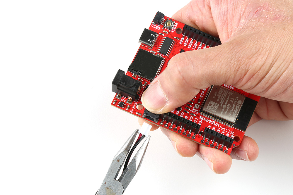
- MEAS — To enable measurements and determine how long your battery might last, we've added a NC (normally closed) jumper between the two MEAS PTH pins. By cutting this jumper, the voltage connecting to the 3.3V voltage regulator input is interrupted. Soldering in a male jumper or wires into the accompanying holes will give you the ability to insert a current meter and precisely monitor how much current your application is consuming.
- PWR — By default, this jumper is closed. Cut this trace to disable the power LED that is connected to 3.3V.
- CHG — By default, this jumper is closed. Cut this trace to disable the charge LED that is connected to the LiPo charge IC.
- LED_D0 — By default, this jumper is closed. Cut this trace to disable the WS2812 addressable RGB LED's output pin labeled as
D0. - JP1 — By default, this jumper is closed. Cut this trace to disable the WS2812 addressable RGB LED's input pin that is connected to pin
14. - JP2 — By default, this jumper is closed. Cut this trace to disable the user LED that is connected to pin
18. - JP3 — By default, this jumper is closed. Cut this trace to disable power connected to the WS2812 addressable LED's 3.3V pin.
- CUR — This three way jumper sets the charge IC's charge rate. By default, it's connected to the pad labeled 500 so the charge rate is set to 500mA. Cutting a trace and adding a solder jumper between the center pad and the pad labeled as 100 will set the charge rate to 100mA.
- I2C — By default, this three-pad jumper is closed and located on the bottom of the board. The three way jumper labeled I2C connect the two 2.2kΩ pull-up resistors to the I2C data and clock lines. If multiple devices are connected to the bus with the pull-up resistors enabled, the parallel equivalent resistance will create too strong of a pull-up for the bus to operate correctly. As a general rule of thumb, disable all but one pair of pull-up resistors if multiple devices are connected to the bus.
- SDPC — By default, this jumper is closed and for the microSD card's power control circuit. Cut this trace on the GND/ON side to disable power to the microSD card's socket. For users that want to control the transistor via a GPIO, add a solder blob between the center pad and the pad that is labeled 17. Make sure to also define the pin in code to toggle power to the microSD card.
 |
 |
| Jumpers Highlighted (Top & Bottom View) |
|
Board Dimensions
The board is 0.9" x 2.3" (22.86mm x 58.42mm) and uses the standard Thing+ footprint. There are 4x mounting holes by each corner of the board. You can use 4-40 standoffs to mount the board to a panel or enclosure.
 |
| Board Dimensions |